


Nanomaterials for Optoelectronics - Group Prof. Dr. Jana Zaumseil
RESEARCH
Our research is mainly focused on the synthesis, characterization and application of nanomaterials for optoelectronic devices. We are particularly interested in charge transport, excitation transfer and light-matter interaction in these materials. We use a wide range of experimental techniques from chemical synthesis, optical spectroscopy (e.g. fluorescence spectroscopy, Raman microscopy etc.), surface characterization (e.g. atomic force microscopy), device fabrication (e.g. under inert conditions, by aerosol jet printing etc.) to electrical and optical device characterization (transport measurements, electroluminescence etc.). For some of our current research topics see below:
Semiconducting Single-Walled Carbon Nanotubes
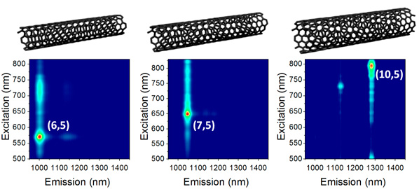
Single-walled carbon nanotubes (SWNTs) are basically rolled-up sheets of graphene. Their diameter (1 - 3 nm) and roll-up vector (n,m) determine their properties, for example, whether they are metallic or semiconducting. They exhibit extremely high thermal and electrical conductivities, outstanding tensile strength and unique optical properties. Networks or thin films of SWNTs are extremely flexible and stretchable without noticeable changes in conductivity. They are environmentally stable and can be processed from dispersions at low temperatures, which makes them suitable for large-area printed circuits on plastic substrates. We are interested in the optical and electronic properties of aligned arrays and random networks of semiconducting SWNTs. We use polymer-wrapping to select specific SWNT chiralities and fabricate field-effect transistors (FETs) based on printed or spincoated networks of nanotubes. These are used to investigate the charge transport and near-infrared light emission properties of such networks.
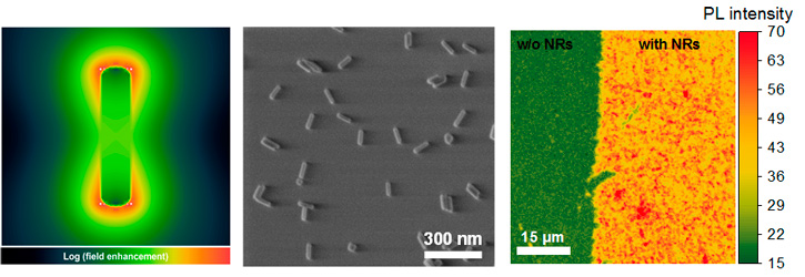
Plasmonic Nanostructures (ERC project EN-LUMINATE)
Solution-processable semiconductors
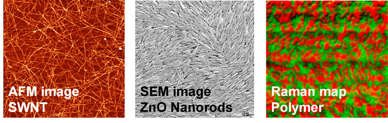
While the vast majority of current electronic circuits and devices is based on silicon and other inorganic semiconductors there is also a large demand for flexible and solution-processable semiconductors for a wide range of applications such as displays, sensors for point-of-care diagnostics etc. A number of novel and unconventional semiconductors are available that are processed from solution or dispersion as thin films such as organic semiconductors (pi-conjugated small molecules or polymers) single-walled carbon nanotubes or semiconducting nanoparticles (e.g. ZnO or PbS). We investigate charge transport and light-emission properties of these materials in order to understand the fundamental mechanisms that govern their performance in optoelectronic devices.
Responsible E-Mail Latest Revision: 05.06.2023